
Date:2019-08-06 Categories:Industry News Hits:639
Printed circuit board {PCB circuit board}, also known as printed circuit board, is the provider of electrical connection of electronic components. Its development has been more than 100 years; its design is mainly layout design; the main advantage of using circuit board is to greatly reduce wiring and assembly errors, improve the level of automation and production labor rate.
According to the number of circuit board layers, it can be divided into single panel, double-sided board, four-layer board, six-layer board and other multi-layer circuit board.
Because printed circuit boards are not general end products, the definition of the name is a little confusing. For example, the motherboard for personal computers is called the motherboard, but not directly called the circuit board. Although there are circuit boards in the main board, they are not the same. Therefore, when evaluating the industry, they are related but not the same. Another example: because there are integrated circuit parts loaded on the circuit board, so the news media call it IC board, but in fact it is not the same as printed circuit board. The printed circuit board we usually refer to the bare board - that is, the circuit board without upper components.
classification
Single panel
On the most basic PCB, parts are concentrated on one side and wires on the other side. Because the wires only appear on one side, this PCB is called single sided. Because the single panel has many strict restrictions on the design of the circuit (because there is only one side, the wiring can not be crossed, and it must take a separate path), so only the early circuits used this kind of board.
Double sided board
This kind of circuit board has wiring on both sides, but to use wires on both sides, it is necessary to have proper circuit connection between the two sides. The "bridge" between these circuits is called a via. A pilot hole is a small hole in a PCB filled with or coated with metal, which can be connected to wires on both sides. Because the area of the double-sided panel is twice as large as that of the single panel, the double panel solves the problem of staggered wiring in the single panel (it can be connected to the other side through the pilot hole), so it is more suitable for more complex circuits than the single panel.
Multilayer board
In order to increase the area that can be wired, the multilayer board uses more single or double-sided wiring boards. The printed circuit board (PCB) with one double-sided as inner layer, two single-sided as outer layer, two double-sided as outer layer, two single-sided as outer layer and two single-sided as outer layer are alternately connected by positioning system and insulating bonding materials, and the conductive patterns are interconnected according to the design requirements, which is also called multilayer printed circuit board. The number of layers of the board does not mean that there are several independent wiring layers. In special cases, empty layers are added to control the thickness of the board. Usually, the number of layers is even and contains the two outermost layers. Most of the motherboards are 4 to 8-layer structure, but in theory, nearly 100 layers of PCB can be achieved. Most of the large supercomputers use a fairly multi-layer motherboard. However, because this kind of computer can be replaced by many ordinary computer clusters, the super multi-layer board has been gradually abandoned. Because the layers in the PCB are closely combined, it is not easy to see the actual number, but if you carefully observe the motherboard, you can still see.
data form
The current circuit board is mainly composed of the following
Pattern: the circuit is used as a tool for conducting between the original parts. In the design, a large copper surface will be designed as the grounding and power layer. Lines and drawings are made at the same time.
Dielectric layer: used to maintain the insulation between lines and layers, commonly known as substrate.
Through hole / via: the through hole can make the lines above two levels connect with each other. The larger through hole is used as the part plug-in. In addition, there are non-conductive holes (npth) which are usually used as surface mounting positioning and fixing screws during assembly.
Solder resist / solder mask: not all copper surfaces need tin parts, so the non tin areas will be printed with a layer of material (usually epoxy resin) to prevent short circuit between non tin eating lines. According to different processes, it can be divided into green oil, red oil and blue oil.
Legend / marking / silk screen: This is an unnecessary component. Its main function is to mark the name and position box of each part on the circuit board, so as to facilitate the maintenance and identification after assembly.
Surface finish: since the copper surface is easy to oxidize in general environment, tin can not be applied (poor solderability), so it will be protected on the copper surface to eat tin. The protection methods include HASL, ENIG, immersion silver, immersion tin, and OSP. Each method has its own advantages and disadvantages, which are collectively referred to as surface treatment.
appearance
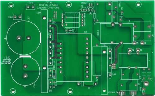
Bare board (without parts on top) is also often referred to as "printed wiring board (PWB)". The substrate of the board itself is made of insulating and non bending materials. The small circuit material that can be seen on the surface is copper foil. Originally, the copper foil was covered on the whole board, but part of it was etched during the manufacturing process, and the remaining part became a network of small wires. These circuits are called conductor patterns, or wiring, and are used to provide circuit connections to parts on a PCB.
Generally, the color of PCB is green or brown, which is the color of solder mask. It is an insulating protective layer, which can protect copper wire, prevent short circuit caused by wave soldering, and save the amount of solder. A silk screen is also printed on the solder mask. It is usually printed with text and symbols (mostly white) to indicate the position of the parts on the board. The screen printing surface is also called a legend.
In the final product, integrated circuits, transistors, diodes, passive components (such as resistors, capacitors, connectors, etc.) and a variety of other electronic components will be installed on it. Through the connection of wires, the electronic signal connection and function can be formed.
advantage
The main advantages of using printed circuit board are as follows:
1. Due to the repeatability (reproducibility) and consistency of the graphics, the wiring and assembly errors are reduced, and the maintenance, debugging and inspection time of the equipment are saved;
2. The design can be standardized, which is conducive to interchangeability; 3. The wiring density is high, the volume is small, and the weight is light, which is conducive to the miniaturization of electronic equipment;
4. It is conducive to mechanized and automatic production, improves labor productivity and reduces the cost of electronic equipment.
PCB manufacturing methods can be divided into subtraction method (subtraction method) and addition method (addition method)