

Date:2019-05-10 Categories:Industry News Hits:570
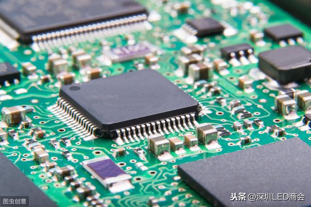
PCB is made of different components and a variety of complex processing technology. The structure of PCB has single-layer, double-layer and multi-layer structure. The manufacturing method of different hierarchical structure is different. (this paper will introduce in detail: the component names and corresponding uses of PCB circuit board, the production of single layer, double layer and multi-layer structure of PCB circuit board and the main functions of various working levels.
1、 The common layer structures of printed circuit boards include single layer PCB, double layer PCB and multi layer PCB. The brief description of these three kinds of layer structures is as follows:
Pad: the metal hole used to weld component pins.
Via: the metal hole used to connect component pins between layers.
Lead wire: copper film of electrical network used to connect component pins.
Filling: used for copper coating of ground wire network, which can effectively reduce the impedance.
Mounting hole: used to fix PCB.
Connector: components used for connection between circuit boards.
Electrical boundary: used to determine the size of the circuit board, all components on the circuit board can not exceed the boundary.
(1) Single layer board: circuit board with copper coating on one side and no copper coating on the other side. Generally, components are placed on the side without copper coating, which is mainly used for wiring and welding. WeChat official account: Shenzhen LED chamber of Commerce
(2) Double layer board: circuit board with copper on both sides, usually called top layer on one side and bottom layer on the other side. Generally, the top layer is used as the surface for placing components, and the bottom layer is used as the welding surface of components.
(3) Multi layer board: a circuit board with multiple working layers. In addition to the top and bottom layers, there are also several intermediate layers. Generally, the intermediate layer can be used as the wire layer, signal layer, power supply layer, grounding layer, etc. Layers are insulated from each other, and the connection between layers is usually realized by via.
2、 Printed circuit board includes many types of working layers, such as signal layer, protective layer, silk screen layer, internal layer, etc
(1) Signal layer: mainly used to place components or wiring. Protel DXP usually consists of 30 intermediate layers, namely mid layer1 ~ mid layer30. The middle layer is used to lay signal wires, and the top and bottom layers are used to place components or copper.
(2) Protective layer: it is mainly used to ensure that the places on the circuit board that do not need tin plating are not tinned, so as to ensure the reliability of circuit board operation. Top paste and bottom paste are top layer and bottom layer respectively; top and bottom Soler are solder paste protective layer and bottom solder paste protective layer respectively.
(3) Screen printing layer: it is mainly used to print the serial number, production number and company name of the components on the printed circuit board.
(4) Internal layer: mainly used as signal wiring layer, PROTEL DXP contains 16 internal layers.
(5) Other layers.