
Date:2018-12-01 Categories:Industry News Hits:568
Printed circuit board, as the substrate of electronic products, has the role of "cornerstone". The dense components on the circuit board must be supported by this, and the most basic electrical performance of electronic products is also based on this.
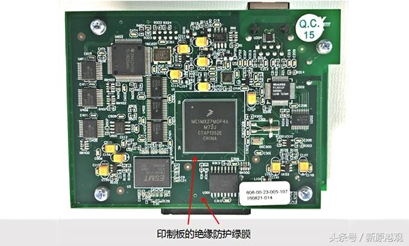
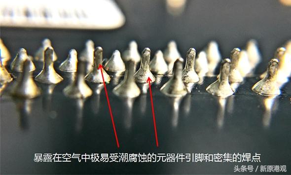
As a printed circuit board, of course, it has the most basic protection technology. The most common one is to apply a layer of high insulation "green film" (or other colors of protective film) on the surface of the printed circuit board. But the most regrettable thing is that all the pins and dense solder joints of the components installed on the printed circuit board are completely exposed to the air, and there is also a lack of appropriate and effective protective measures, which will inevitably lead to printing Board making and its components are damaged by moisture, harmful gas and salt fog in the air, resulting in the oxidation, corrosion and ion migration of components, and even the electrical performance of printed circuit board is reduced. Although the common coating process of three proofing paint can play a certain role of moisture and corrosion protection, it can not meet the requirements of printing due to its own shortcomings and limitations The basic requirements of plate protection.
Nowadays, the development trend of printed circuit board is towards high density, high precision, fine aperture, thin wire, fine pitch, high reliability, multilayer, high speed transmission, light weight and thin shape. Therefore, higher and higher performance requirements are put forward for PCB. However, one of the biggest obstacles to meet the above requirements is the limitation of "electrical clearance" and "creepage distance", which greatly increases the difficulty of reducing the cost of electrical materials.
Nowadays, electronic deep protection technology can provide strong technical support and guarantee for effectively solving the above problems.
The electronic depth protection agent with the function of "quantum tunnel conduction" can be directly applied to the metal surface of all components on the printed circuit board. The protective agent forms a close and firm chemical bond with the metal surface, which is like a very thin protective layer which can automatically select "conductive" and "insulation" on the metal surface, so as to ensure the metal lead of electronic components The good conductivity of a large number of metal solder joints on the foot and printed circuit board ensures the overall insulation of the printed board, which solves the "defect" problem mentioned above.
The biggest advantage of electronic deep protection technology is that it can well meet the requirements of the development trend of printed circuit board on the electrical performance of printed circuit board
1. Resistance to ion migration
Ion migration is the phenomenon that the conductive wire grows along the surface of glass fiber between the two positive and negative electrodes of printed circuit board, which leads to the insulation damage. The electronic depth protector coated on the printed circuit board can isolate the growth path of the conductive wire, so that the printed circuit board has good resistance to ion migration.
2. Achieve high reliability of insulation and conductivity of printed circuit board
The resistance coefficient of the electronic depth protector is as high as 10g Ω, but the protective agent can conduct electricity well under the contact pressure of the electrical contact, and its conductivity is better than that of copper, which makes the insulation and conductivity of printed circuit board get "bidirectional" improvement.
3. It is conducive to the thinness of PCB
Due to its good electrical properties, EPD not only has good insulation and conductivity, but also has a strong and environmentally friendly coating. It also has good high frequency characteristics, solderability and mechanical properties. Its protective film is also very thin (only about 1 μ m), which can bring the following benefits to PCB:
1) It is conducive to the light weight of electronic products;
2) It is beneficial to eliminate electromagnetic signal interference;
3) It is conducive to high-speed signal transmission;
4) It can reduce the dielectric constant and improve the signal transmission speed;
5) It is conducive to the high-density production of thin copper foil circuit and reduces the side corrosion phenomenon;
6) It is beneficial to the production of thin copper foil transmission line and improve the characteristic impedance.