
Date:2018-11-09 Categories:Industry News Hits:618
1、 What is aluminum substrate
PCB is printed circuit board, also known as printed circuit board.
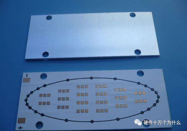
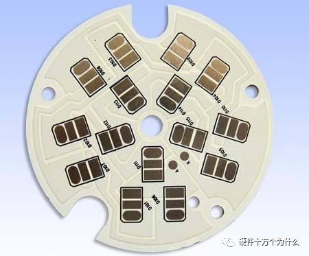
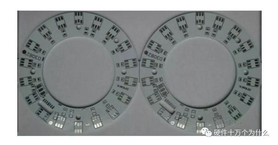
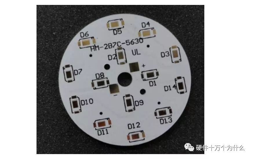
Aluminum substrate is a kind of PCB
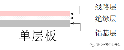
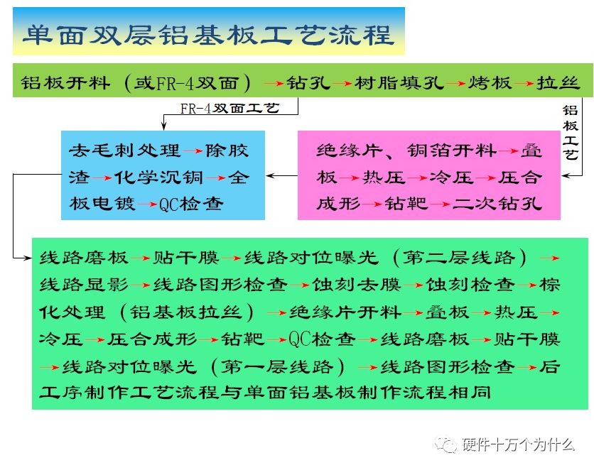
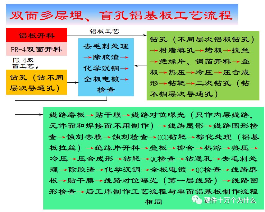
Aluminum substrate is a kind of metal based copper clad laminate with good heat dissipation function. Generally, the single panel is composed of three layers: circuit layer (copper foil), insulation layer and metal base layer. For high-end use, there are also double-sided boards, the structure is circuit layer, insulation layer, aluminum base, insulation layer, circuit layer. Very few applications are multi-layer boards, which can be made of ordinary multilayer boards, insulation layer and aluminum base.
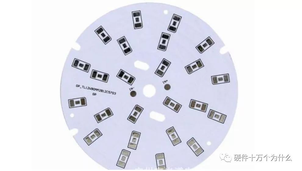
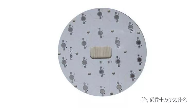
Single side aluminum substrate: there is only one layer of conductive pattern layer and insulating material plus aluminum plate (substrate).
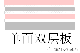
Double sided circuit aluminum substrate: there are two layers of conductive pattern layer superimposed with insulating material plus aluminum plate (base plate).
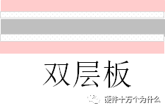
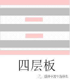
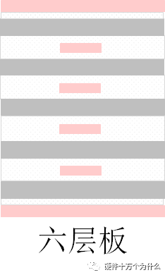
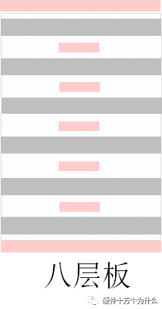
Multilayer printed aluminum based circuit board: printed circuit board made of three or more conductive pattern layers and insulating material plus aluminum plate (substrate) alternately laminated and bonded together.
According to the surface treatment method:
Gold plate (chemical thin gold, chemical thick gold, selective gold precipitation)
Electrogold plate (full board electrogold finger selective electrogold)
Tinplate
Silver plate
Electric silver plate
Palladium plate
2、 Working principle of aluminum substrate
The surface of the power device is mounted on the circuit layer, and the heat generated during the operation of the device is quickly transferred to the metal base layer through the insulation layer, and then the heat is transferred out by the metal base layer, so as to realize the heat dissipation of the device (see Fig. 2).
Compared with the traditional FR-4, the aluminum substrate can reduce the thermal resistance to the minimum, so that the aluminum substrate has excellent thermal conductivity; compared with the thick film ceramic circuit, its mechanical properties are excellent.
In addition, aluminum substrate has the following unique advantages:
Meet ROHS requirements;
It is more suitable for SMT process;
In the circuit design scheme, the thermal diffusion is treated effectively to reduce the operating temperature of the module, prolong the service life, and improve the power density and reliability;
Reduce the assembly of radiator and other hardware (including thermal interface materials), reduce product volume, reduce hardware and assembly costs, optimize the combination of power circuit and control circuit;
Replace fragile ceramic substrate for better mechanical durability.
3、 Composition of aluminum substrate
1. Line layer
The circuit layer (usually electrolytic copper foil) is etched to form printed circuit, which is used to realize the assembly and connection of devices. Compared with the traditional FR-4, the aluminum substrate can carry higher current with the same thickness and line width.
2. Insulating layer
Insulation layer is the core technology of aluminum substrate, which mainly plays the functions of bonding, insulation and heat conduction. Aluminum substrate insulation is the largest thermal barrier in power module structure. The better the thermal conductivity of the insulation layer is, the more conducive to the diffusion of heat generated during the operation of the device, and the more conducive to reducing the operating temperature of the device, so as to improve the power load of the module, reduce the volume, prolong the life, and improve the power output.
3. Metal base
What kind of metal is used for insulating metal substrate depends on the comprehensive consideration of thermal expansion coefficient, thermal conductivity, strength, hardness, weight, surface state and cost of the metal substrate.
4、 Performance of aluminum substrate
1、 Heat dissipation
At present, many double-sided boards and multilayer boards have high density, high power and difficult heat dissipation. Conventional printed circuit board substrates such as FR4 and cem3 are poor thermal conductors, insulation between layers, heat can not be emitted. Local heating of electronic equipment cannot be ruled out, which leads to high temperature failure of electronic components. Aluminum substrate can solve this heat dissipation problem.
2、 Thermal expansion
Thermal expansion and cold contraction are the common nature of materials, and the coefficient of thermal expansion of different substances is different. Aluminum based printed circuit board can effectively solve the problem of heat dissipation, so as to alleviate the thermal expansion and cold contraction of different components on the printed circuit board, and improve the durability and reliability of the whole machine and electronic equipment. Especially solve the problem of SMT (surface mount technology) thermal expansion and cold contraction.
3、 Dimensional stability
Aluminum based printed boards, obviously, are much more stable in size than printed boards made of insulating materials. From 30 ℃ to 140 ~ 150 ℃, the dimension of aluminum based printed board and aluminum sandwich board is 2.5 ~ 3.0%
4、 Other reasons
Aluminum based printed circuit board has shielding effect, replaces brittle ceramic substrate, uses surface mounting technology at ease, reduces real effective area of printed board, replaces radiator and other components, improves heat resistance and physical properties of products, and reduces production cost and labor.
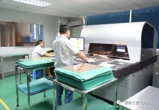
5、 Manufacturing process of aluminum substrate
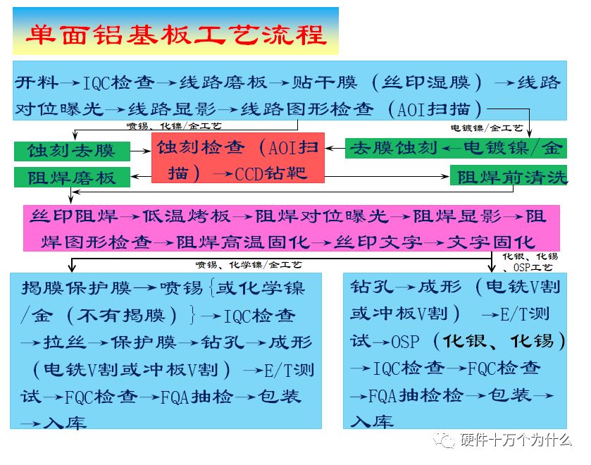
1) Cutting
1. Opening process
Incoming material → cutting material → baking plate
Incoming material: the raw material for Aluminum Based PCB production, also known as aluminum based copper clad laminate, is formed by pressing heat conducting material or semi cured sheet and copper foil on aluminum plate.
Cutting: cutting is the process of cutting a large piece of material into small pieces by machine according to the requirements of different panels. After cutting, the edge of the plate is sharp, which is easy to scratch the hand, and at the same time, it makes the plate and the plate scratch. Therefore, the edge is grinded by the edger after cutting.
Baking board (baking board)
1. Baking purpose:
① . eliminate the internal stress produced in the production of sheet metal.
Improve the dimensional stability of materials
② . remove moisture absorbed by sheet metal during storage,
Increased reliability of materials.
2. Baking conditions:
Bake the plate at 150 ℃ for 4 hours. The thickness of the laminated plate is usually 50 cm
A pile of rice
2. Purpose of cutting
Cut the large size incoming material into the required size for production
3. Notes on cutting
① Check the size of the first piece after opening the material
② Pay attention to aluminum and copper scratches
③ Pay attention to the delamination and edge of plate edge
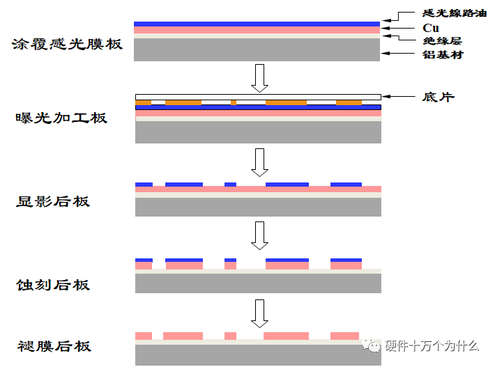
2) Dry / wet film imaging
Wet film (also known as photosensitive circuit oil) and photosensitive dry film are all photosensitive materials. When the material encounters ultraviolet light, it will polymerize to form a relatively stable image, and will not dissolve in weak alkali, while the non photosensitive part will dissolve in weak alkali.

1. Dry / wet film imaging process
Grinding - Film - exposure - Development
2. Purpose of dry / wet film imaging
The parts needed to make the circuit are shown on the sheet metal
3. Precautions for dry / wet film imaging
① Check whether there is an open circuit in the circuit after developing
② Whether there is deviation in developing alignment to prevent dry film breakage
③ Pay attention to the poor circuit caused by the scratch on the board surface
④ There should be no residual air during exposure to prevent poor exposure
⑤ After exposure, it is necessary to stand still for more than 15 minutes before developing
Exposure:
The function of exposure is that the ultraviolet light of the exposure machine makes part of the pattern on the film sensitive through the negative film, thus transferring the pattern to the copper plate.
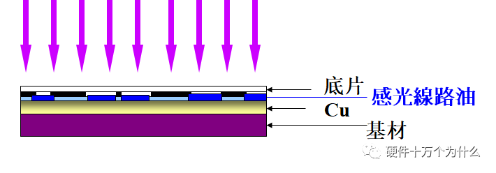
development:
The function of development is as follows
Is to remove the unexposed part of the dry film, leaving the photosensitive part.
Development principle:
The photosensitive material in the unexposed part did not polymerize and dissolved in weak base Na2CO3 (0.8-1.2%). The polymerized photosensitive material is left on the plate surface to protect the copper surface from being dissolved by etching solution.

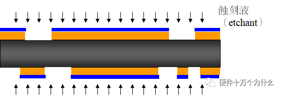
3) Acid / alkaline etching
1. Acid / alkaline etching process
Etching stripping drying inspection
2. Acid / alkaline etching purpose
After the dry / wet film is imaged, the required circuit part is reserved, and the surplus part except the line is removed
3. Precautions for acid / alkaline etching
① Pay attention to the unclean etching and excessive etching
② Pay attention to line width and line thickness
③ Oxidation and scratch are not allowed on copper surface
④ The drying film should be removed completely
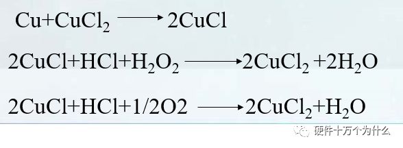
Function of etching:
It's etching the copper side of the unexposed part.
4) Melatonin

The film on the copper surface of the protection line is removed by high concentration of NaOH (3-5%). The concentration of NaOH solution should not be too high, otherwise it is easy to oxidize the board surface.
5) AOI process
The principle of the machine is to use the reflection of copper surface to make the graphics on the board can be scanned by AOI and recorded in the software, and compared with the data and graphics provided by customers to check the defect points. Such as open circuit, short circuit, poor exposure and other defects can be detected through AOI machine.
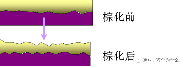
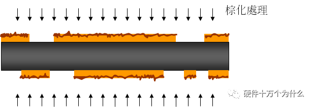
6) Browning
The function of browning process is to roughen the copper surface, increase the bonding area and increase the surface bonding force.
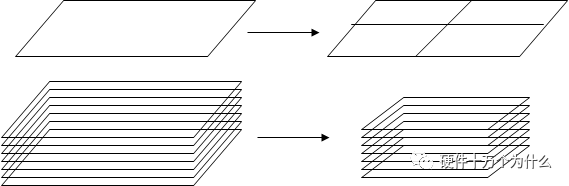
7) Pressure plate
Process introduction: the pressing plate is to connect the outer copper foil and the inner layer, as well as the inner layer and the inner layer into a whole to form a multilayer board.
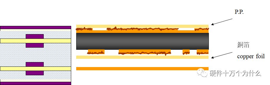
Process principle: according to the characteristics of the semi curing sheet, it melts at a certain temperature and becomes a liquid state to fill the graphic space and form an insulating layer. Then it is further heated and gradually solidified to form a stable insulating material. At the same time, each layer of the circuit is connected into a whole multilayer board.
What is prepreg?
Prepreg is the abbreviation of pre giant. It is a kind of sheet bonding material synthesized by resin and glass fiber carrier.
Resin - usually a polymer, a thermosetting material. At present, epoxy resin FR-4 is commonly used.
Outer layer pre process
8) Drilling
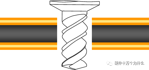
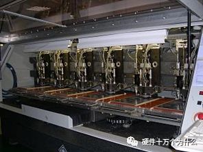
1. Drilling process
Pin drilling inspection board
2. Purpose of drilling
The positioning drilling of the plate can assist the subsequent production process and customer assembly
3. Precautions for drilling
① Check the number of boreholes and the size of empty holes
② Avoid scraping of sheet metal
③ Check the edge of aluminum surface and hole position deviation
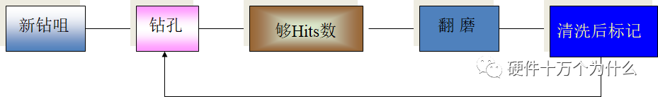
④ Check and replace the drill bit in time
⑤ Drilling is divided into two stages, one is drilling: after cutting, the drilling is peripheral tool hole;
Second drill: tool hole in the unit after resistance welding
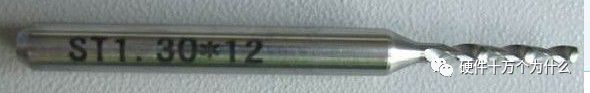
Features of drill bit for aluminum substrate
① Large chip removal space of bit: small chip removal resistance, smooth chip removal, small heat generated by drilling, and reduced drilling pollution;
② Extraordinary cutting edge sharpness: due to the use of nanotechnology and advanced grinding technology, the cutting edge of the drill bit is sharper than before, which can reduce the cutting force, reduce the broken drilling rate and improve the quality of hole wall;
③ Tool design based on customer application: there are a variety of drill bits, which can meet different application requirements. All parameters of the bit, such as core thickness and core taper, have been carefully designed with obvious effectiveness;
④ The cutting edge is strictly symmetrical: it is conducive to efficient cutting and avoid drilling offset.
9) Copper plating
A layer of conductive metal is deposited in the hole of the board after drilling by chemical method, and the metal layer is thickened by electroplating on the whole plate, so as to achieve the purpose of metallization in the hole and make the circuit connected
technological process:
Plate grinding → rubber slag removal → copper deposition → whole plate electroplating → next process
Electroless copper deposition, commonly known as copper deposition, is a kind of autocatalytic chemical oxidation and reduction reaction. In the process of electroless copper plating, Cu2 + ion is reduced to metal copper by electrons, and the reducing agent emits electrons, which is oxidized. Electroless copper plating is used for hole metallization in PCB manufacturing to connect the wires between double-sided boards and multi panel layers.
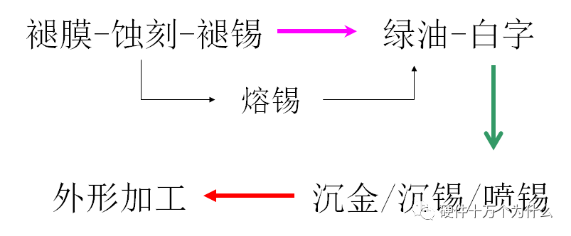
5) Screen printing solder mask, character
1. Silk screen solder mask, character flow
Screen printing - pre baking - exposure - Development - characters
2. Purpose of screen printing solder mask and characters
① Anti soldering: protect the circuit without soldering tin to prevent the tin from entering and causing short circuit
② Character: to mark
3. Matters needing attention of solder mask and character in silk screen printing
① Check whether there is garbage or foreign matter on the board surface
② Check the cleanliness of the mesh plate
③ After screen printing, pre bake for more than 30 minutes to avoid bubbles in the circuit
④ Pay attention to the thickness and uniformity of silk screen printing
⑤ After pre baking, the plate should be completely cooled to avoid touching the film or damaging the glossiness of the ink surface
⑥ When developing, the ink side should be placed downward
6) V-CUT, Gong board
1. V-CUT, process of gongs and boards
V-CUT -- Gong board -- tear off protective film -- remove the edge
2. V-CUT, purpose of Gong board
① V-CUT: the single PCs line is connected with the whole PNL plate cutting, leaving a small part connected to facilitate packaging and taking out
② Gong board: remove the redundant part of circuit board
3. Notes on V-CUT and Gong board
① In the process of V-CUT, attention should be paid to the size of V, the incomplete edge and burr
② Pay attention to the burr and skew of the gongs. Check and replace the gongs in time
③ Finally, in addition to the front to avoid scratch
7) Testing, OSP
1. Test, OSP process
Line test - withstand voltage test - OSP
2. Test, OSP purpose
① Circuit test: check whether the completed circuit works normally
② Withstand voltage test: test whether the completed line can withstand the specified voltage environment
③ OSP: better soldering of the circuit
3. Test, OSP considerations
① How to distinguish between qualified and unqualified products after testing
② Post OSP placement
③ Avoid line damage
8) FQC, FQA, packaging, shipping
1. Process
FQC - FQA - Packaging - shipment
2. Purpose
① FQC shall conduct full inspection and confirmation for the products
② FQA spot check and verification
③ Package and ship to customer as required
6、 Application of PCB aluminum substrate
1. Audio equipment: input and output amplifier, balanced amplifier, audio amplifier, preamplifier, power amplifier, etc.
2. Power supply equipment: switch regulator, DC / AC converter, SW regulator, etc.
3. Communication electronic equipment: high frequency amplifier, filter and transmission circuit.
4. Office automation equipment: motor driver, etc.
5. Automobile: electronic regulator, igniter, power controller, etc.
6. Computer: CPU board, floppy disk drive, power supply device, etc.
7. Power module: converter, solid state relay, rectifier bridge, etc.
8. Lamp decoration: with the promotion of energy-saving lamps, aluminum substrates used in LED lamps have also begun to be widely used.