

Date:2018-05-29 Categories:Industry News Hits:501
1. When the output data of solder mask is generated, there is no need to increase or compensate the solder pad.
It is better to leave the solder pad on the same size as the copper pad. Then, we will set up the solder mask to meet the technical requirements of the correct production and assembly of the circuit board.
The preferred version without oversize is worse: the gasket is too large

2. Preparation rules of solder resist used by us:
We set the value of solder mask preparation according to the PCB pattern category. Different functions are shown in the figure:
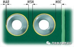
Mar (mask ring) - gap between solder mask and copper pad
MSM (mask segment) - solder bridge between adjacent pads
MOC (mask overlap gap) - a solder mask between a track or plane and an adjacent solder mask window
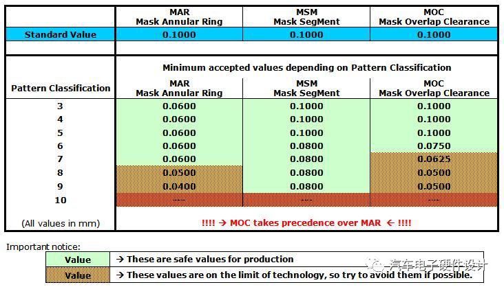
We always apply the standard values to the complete solder mask. According to the design, we can reduce these standard values at specific locations to the minimum acceptable value to generate the best solder mask.
The standard values of Mar, MSM and MOC of all patterns were 0.1000mm (4mil).
The minimum acceptable values for Mar, MSM and MOC depend on the schema classification according to the table below (values in mm only)
Important:
If the mask segment (MSM) between masks is less than 0.0800mm (3.15mil), it will be removed as a mask segment less than 0.080mm (3.15mil). If the mask fragment (MSM) is less than 0.080mm (3.15mil)

For npth bits without copper pads, the mask ring (MAR) is always 0.125 mm (4.92 mil) regardless of pattern grade.
3. Concave via: the copper pad of through-hole is covered by solder mask.
When we spray all our solder mask, technical support does not mean that the through hole is completely closed or covered with solder mask.
Complete closure of the through hole can only be guaranteed by using viafilling (see viafilling section below)
Important: if you need to support vias, make sure that the solder mask data you generate does not have a solder pad for the vias.
4. Npth hole without copper pad should always be provided with welding pad clearance pad.
5. When the output is generated, the circuit board contour is included in the solder mask. It is best to use a small line - for example, 0.50 mm (20 mil) wide - with the center of the line being the exact outline of the board. We will remove the line from the final production preparation data.
Important: if you need no solder mask in the PCB edge area, use thick lines to indicate the board outline. The line width should be at least 2.00 mm (79 mil) to produce a 1.00 mm (39.5 mil) boundary without solder mask. It is also recommended to point out solder free frames in the mechanical plan.