

Date:2018-05-29 Categories:Industry News Hits:652
PCB overview
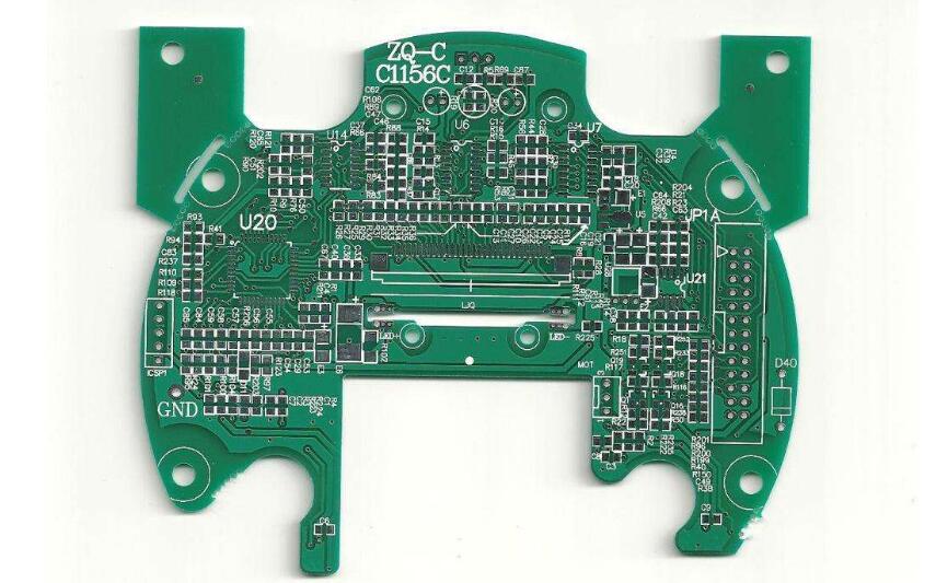
Printed circuit board (PCB), which is also known as printed circuit board (PCB) in Chinese, is an important electronic component, the support of electronic components and the carrier of electrical connection of electronic components. Because it is made by electronic printing, it is called "printed" circuit board.
General principles of PCB design
In order to get the best performance of electronic circuit, the layout of components and wires is very important. In order to design PCB with good quality and low cost, the following general principles should be followed.
(1) Special component layout
First of all, we should consider the size of PCB: if the PCB size is too large, the printing line will be long, the impedance will increase, the anti noise ability will be reduced, and the cost will also increase; if the PCB size is too small, the heat dissipation will not be good, and the adjacent lines will be easily disturbed. After determining the PCB size, determine the position of special components. Finally, according to the functional unit of the circuit, all components of the circuit are arranged.
When determining the location of special components, the following principles should be observed:
① As far as possible to shorten the connection between high-frequency components, try to reduce their distribution parameters and mutual electromagnetic interference. Components susceptible to interference shall not be too close to each other, and input and output components shall be kept away from each other as far as possible.
② There may be high potential difference between some components or wires, so the distance between them should be increased to avoid accidental short circuit caused by discharge. The components with high voltage should be arranged in the place where hands are not easy to touch during debugging.
③ Components weighing more than 15g should be fixed with bracket and then welded. Those large, heavy and heat generating components should not be installed on the printed board, but should be installed on the chassis bottom plate of the whole machine, and heat dissipation should be considered. The thermistor should be away from the heating element.
④ For the layout of potentiometer, adjustable inductance coil, variable capacitor, micro switch and other adjustable components, the structural requirements of the whole machine should be considered. In case of internal adjustment, it should be placed on the printed board where it is convenient to adjust; if it is adjusted outside the machine, its position should be adapted to the position of the adjusting knob on the chassis panel.
⑤ Set aside the position occupied by positioning hole and fixing bracket of printed board.
(2) General component layout
According to the functional unit of the circuit, the layout of all components of the circuit shall comply with the following principles:
① The position of each functional circuit unit is arranged according to the circuit flow, so that the layout is convenient for the signal flow, and the signal is as consistent as possible.
② With the core components of each functional circuit as the center, the layout is carried out around it. Components should be evenly, neatly and compactly arranged on PCB to minimize and shorten lead wires and connections between components.
③ The distributed parameters between components should be considered when the circuit works at high frequency. In general, the components should be arranged in parallel as far as possible, so that it is not only beautiful, but also easy to assemble and weld, and easy to mass produce.
④ For components located at the edge of circuit board, the distance from the edge of circuit board shall not be less than 2mm. The best shape of circuit board is rectangle. The aspect ratio is 3:2 or 4:3. When the size of circuit board is greater than 200 mm × 150 mm, the mechanical strength of circuit board should be considered.
(3) Wiring
The principle of wiring is as follows:
① The wires for input and output terminals should avoid adjacent parallel as far as possible, and it is better to add ground wire between lines to avoid feedback coupling.
② The minimum width of printed board wire is mainly determined by the adhesion strength between the conductor and the insulating substrate and the current value flowing through them. When the thickness of copper foil is 0.5mm and the width is 1-15mm, the temperature rise will not be higher than 3 ℃ through 2A current. Therefore, the wire width of 1.5mm can meet the requirements. For integrated circuits, especially digital circuits, 0.02-0.3mm wire width is usually selected. Of course, as long as it is allowed, wide wires, especially power and ground wires, should be used as far as possible. The minimum spacing of conductors is mainly determined by the insulation resistance and breakdown voltage in the worst case. For integrated circuits, especially for digital circuits, the spacing can be less than 0.1 ~ 0.2mm as long as the process permits.
③ The bend of printed wire is generally circular arc, and the right angle or included angle will affect the electrical performance in high frequency circuit. In addition, try to avoid using large area copper foil, otherwise, when heated for a long time, the copper foil will expand and fall off. When a large area of copper foil must be used, it is better to use grid shape, which is conducive to eliminating volatile gas generated by the heating of adhesive between copper foil and substrate.
(4) Pad
The center hole of the pad is slightly larger than the lead diameter of the device. If the pad is too large, it is easy to form false soldering. The outer diameter D of the pad is generally not less than (D + 1.2) mm, where D is the lead hole diameter. For high density digital circuits, the minimum pad diameter can be (D + 1.0) mm.
What subjects need to be learned when designing PCB
To design and design PCB circuit board, first of all, we should know the basic electronic basis, component knowledge, drawing software operation, and understand part of the programming process. In addition, design software needs to know some knowledge of electromagnetic compatibility.
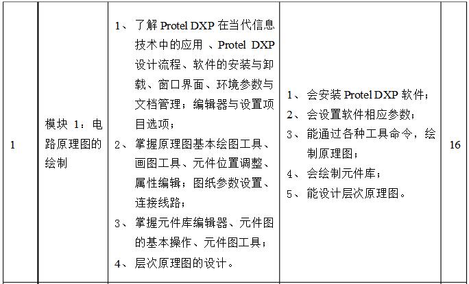
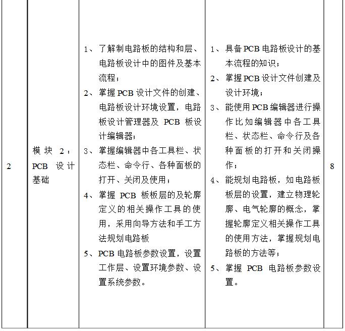
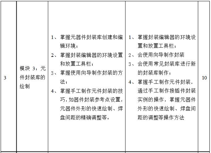
Contents and requirements of PCB Design Course

Six PCB design books
1. Design and fabrication of Protel99SE multilayer circuit board
2. Advanced application of portal 99SE (Revised Edition) compiled by Zhao Jingbo
3. "Altium designer PCB Sketchpad (with video)" written by Zheng Zhenyu Kivy
4. PCB design compendium
This book introduces how to use OrCAD software package to design and produce printed circuit board. A large number of examples in the book show how to use capture to draw circuit schematic diagram, and how to design circuit boards that can be put into production with pcbeditor. At the same time, it also describes the related knowledge of PCB design, including PCB production process, reference standards, producibility design, signal integrity design, etc. This book can not only be used as a test book for college students and engineers to learn the software, but also as a reference book for understanding the design process of printed circuit board.
5. Design and manufacture of PCB board
The design and production of PCB is explained with Protel 2004 Chinese version. It focuses on the design of schematic diagram, PCB board and component library, and briefly introduces some basic operation methods and skills of handmade printed circuit board. The book language is simple, easy to understand, comprehensive and specific knowledge points, is the editor of many years engaged in printed circuit board experience. Through a large number of design examples, this paper illustrates some skills and methods in schematic design and PCB design, as well as the problems that should be paid attention to in the design process. It is good in engineering and practical. PCB design and production can be used as teaching materials for electronic information engineering, communication engineering, automation, electrical and computer application in higher vocational colleges. It can also be used as a self-study teaching material for circuit design enthusiasts, a training textbook for social training classes and a teaching material for Protel circuit design certification assessment. This book is edited by Xia Shuli and Zhang Jiangwei of Xuzhou Institute of technology.